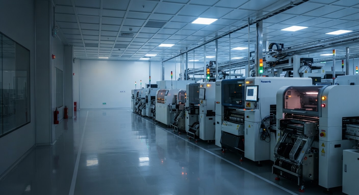
Full-spectrum electronics manufacturing services — from schematic capture and PCB layout through SMT assembly, conformal coating, and box-build integration. 30,000 m² of production floor with eight high-speed SMT lines running 24/7 across two shifts, delivering over 2.8 million placements per hour of aggregate throughput.
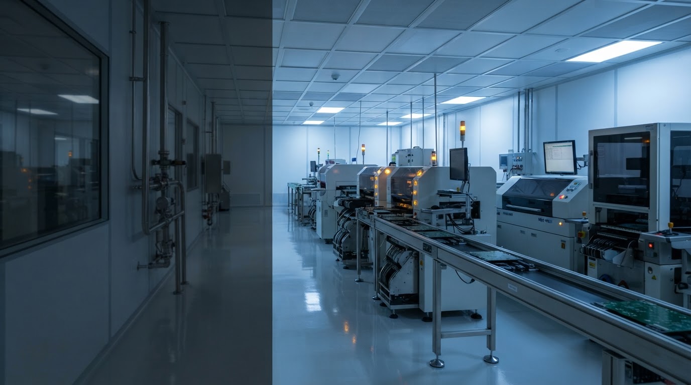
MRYK Group operates one of the largest integrated PCBA facilities serving the Belt and Road corridor. Our Shenzhen campus combines R&D engineering, new product introduction, volume SMT production, through-hole assembly, testing, and logistics within a single secured compound — eliminating the handoff friction that plagues multi-vendor supply chains.
Every PCB we produce passes through a gated quality process spanning automated solder paste inspection, pre- and post-reflow AOI, flying-probe and bed-of-nails ICT, and functional testing against customer-approved test plans. Our engineering team brings an average of 12 years of DFM experience across consumer, industrial, automotive, and medical device verticals.
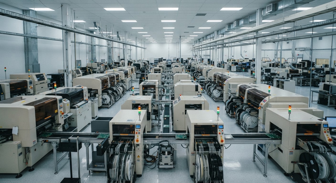
Our production lines are configured to handle the full complexity spectrum — from simple single-sided consumer boards to high-density interconnect multilayer stacks with blind and buried vias.
Additional capabilities including blind and buried vias, via-in-pad, edge plating, peelable solder mask, carbon ink, and custom stack-ups are available on request. Contact our engineering team for a full capability matrix aligned to your project requirements.
Our engineering teams specialize in translating demanding application requirements into manufacturable PCB designs, with deep domain expertise across three core verticals.
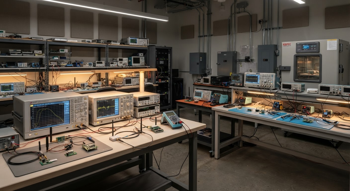
High-density interconnect boards for wearables, smart-home devices, sensor nodes, and connected appliances. We support rigid, flex, and rigid-flex stacks with miniaturized footprints down to 0201 passives and 0.35 mm pitch BGAs. Our quick-turn prototyping line enables iteration cycles measured in days, not weeks.
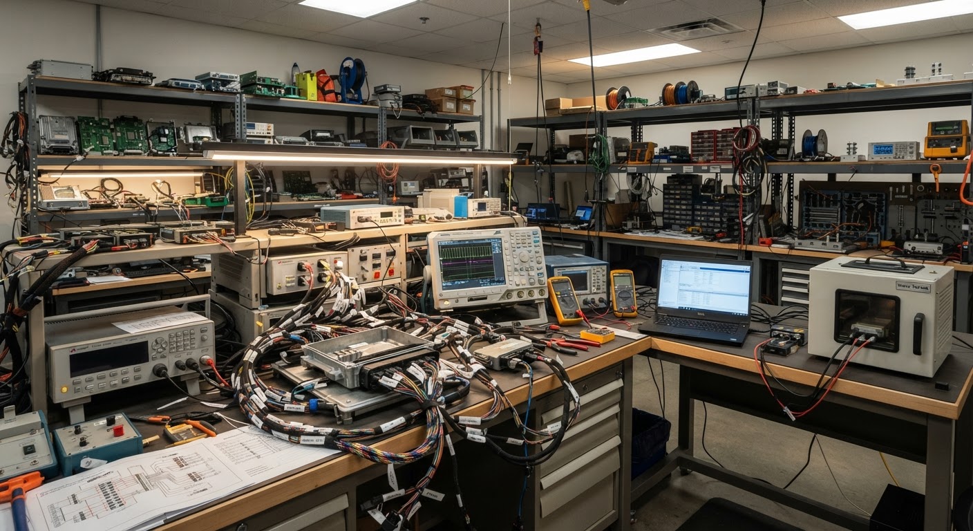
IATF 16949-certified production for body control modules, LED lighting drivers, battery management systems, infotainment, and ADAS sensor interfaces. We handle heavy copper (up to 6 oz), controlled impedance, high-temperature substrates, and full traceability per PPAP Level 3 requirements.
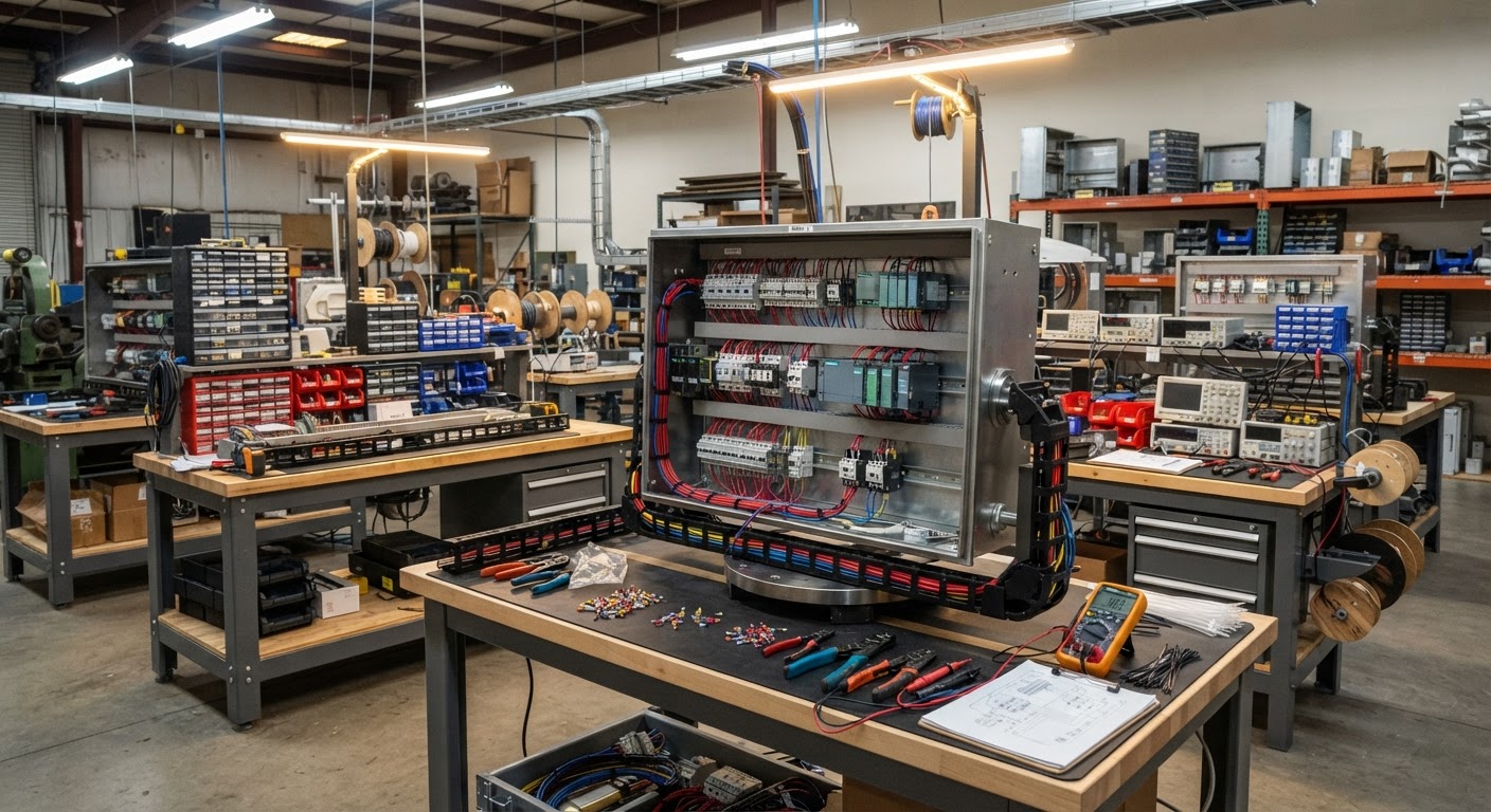
Robust boards for motor drives, PLCs, industrial power supplies, inverter stages, and DIN-rail automation modules. We provide conformal coating, potting, thermal pad bonding, and functional end-of-line testing under extended temperature ranges. Designs routinely incorporate isolation barriers, creepage management, and high-current bus structures.
Electronics manufacturing is only one link in the value chain. Explore complementary capabilities that turn a bare PCB into a fielded, connected product.
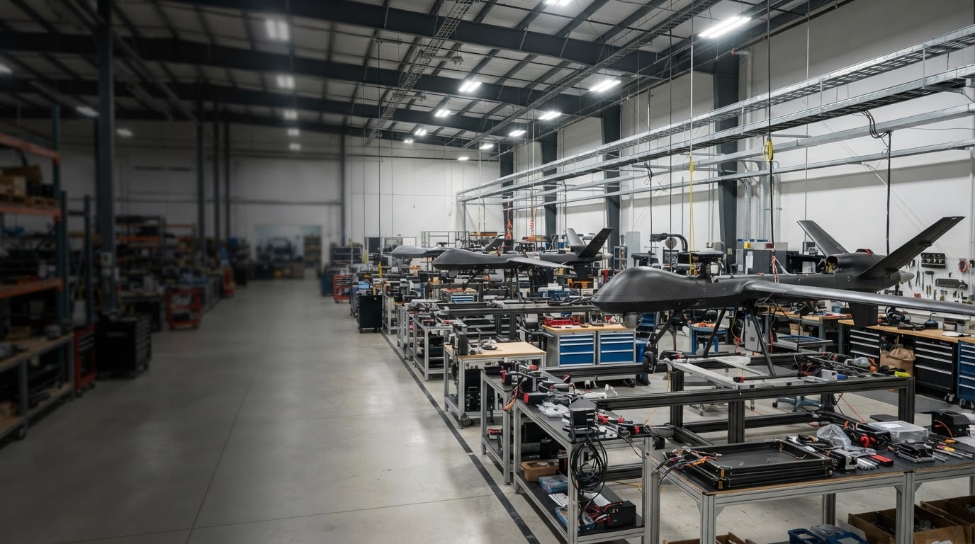
Flight controllers, ESC modules, telemetry radios, and payload interfaces — the PCBA backbone of commercial UAV platforms, designed and assembled in-house.
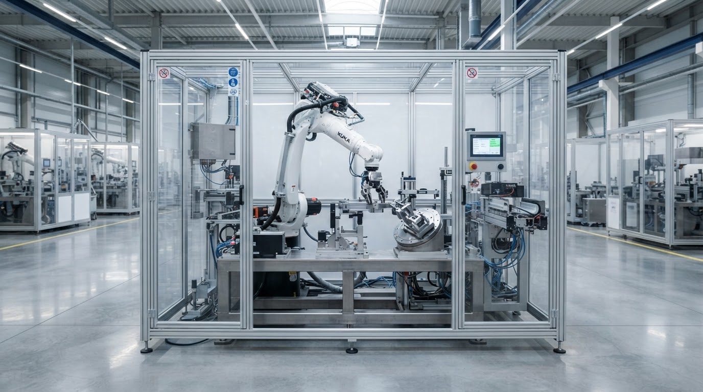
Servo drive boards, sensor fusion modules, and real-time control systems — the embedded electronics that power industrial and collaborative robots.
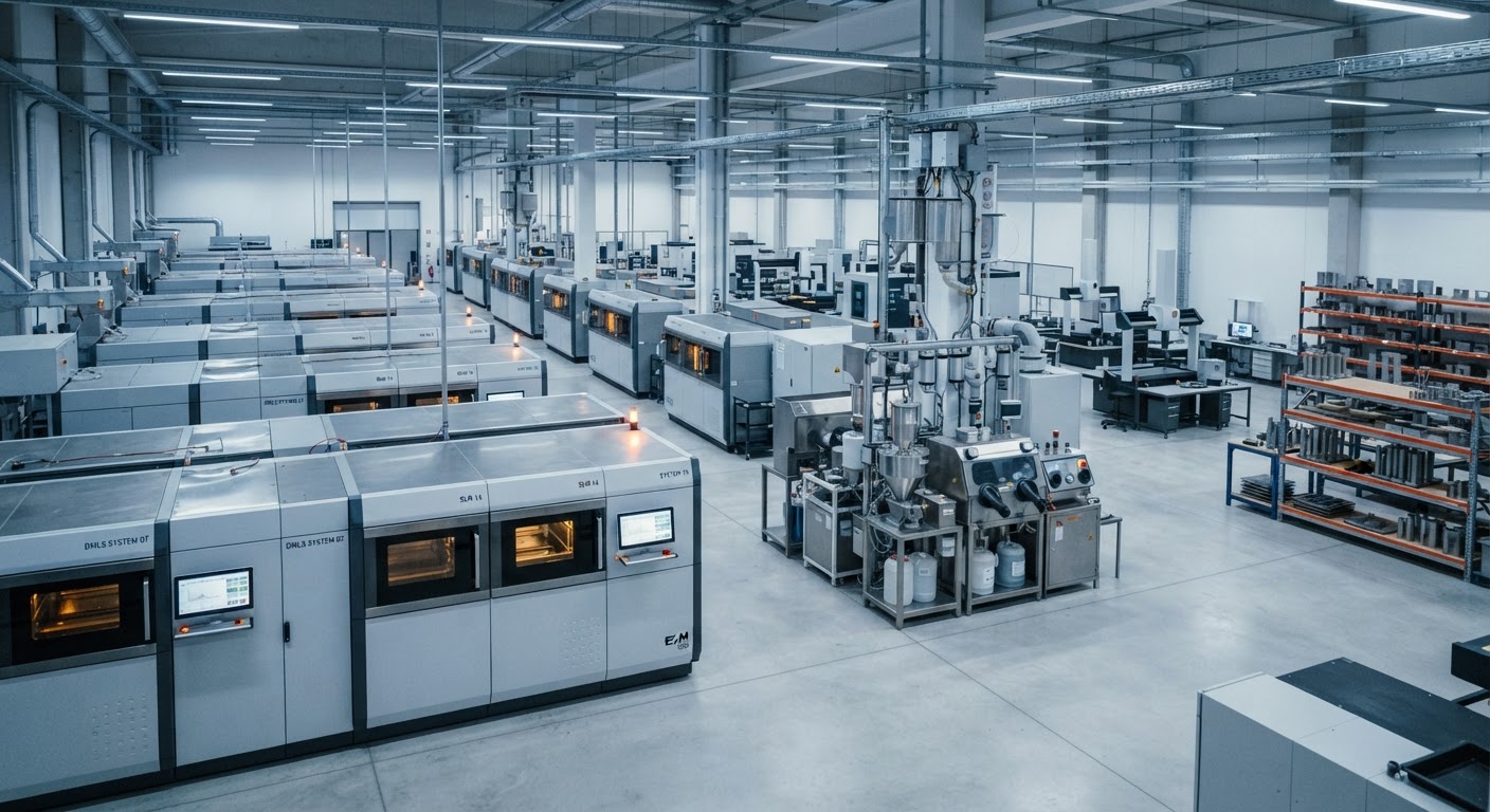
Additive manufacturing for enclosures, thermal management structures, and production jigs — complementing electronics builds with rapid in-house mechanical parts.

Whether you need a 72-hour prototype turnaround on a 4-layer IoT board or a 100,000-unit automotive production ramp with full PPAP documentation — our engineering and commercial teams are ready to engage. Share your Gerber files, BOM, and target quantity for a same-day feasibility review and quotation.